PCB Manufacturing: The State of Optical Metrology
Advanced metrology solutions for modern printed circuit board manufacturing processes.
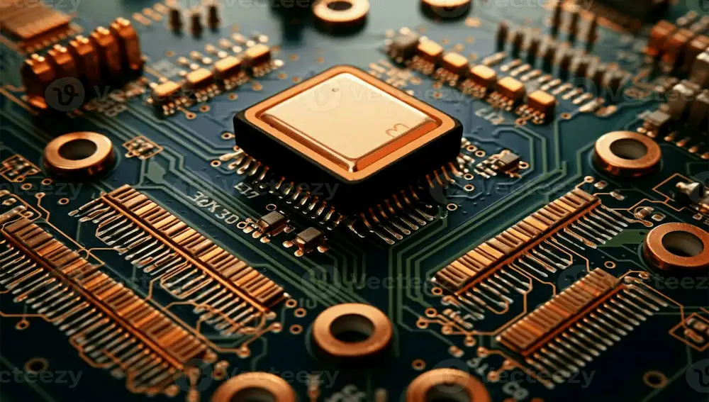
In modern electronics manufacturing, printed circuit boards (PCBs) have evolved into complex, multilayered platforms supporting high-density interconnects, microvias, and ultra-fine trace geometries. Ensuring dimensional integrity at this scale is critical—not only for electrical performance but also for downstream assembly, thermal reliability, and regulatory compliance.
While optical metrology has become the industry's preferred approach for non-contact inspection, it still faces key limitations in high-mix production environments:
Common Challenges in PCB Optical Inspection
Manual Programming Bottlenecks:
Most systems still rely on time-consuming, manual feature selection and alignment workflows, which scale poorly with diverse board types.
Limited CAD Integration:
Inspection systems often operate in isolation from upstream design tools, forcing duplication of effort and increasing the risk of oversight.
Rigid Standards Support:
Some equipment lacks flexibility to support different international dimensional standards or composite fitting benchmarks.
Measurement Throughput:
High-resolution imaging over large boards with thousands of features can lead to long cycle times—especially when multiple machines are required.
Complex Feature Interpretation:
Features like curved traces, irregular pads, or gold-powdered terminals present challenges for traditional edge-detection and measurement algorithms.
Where the Industry Lags
Despite advances in imaging hardware, many PCB inspection tools are constrained by legacy software architectures that limit their adaptability, automation potential, and integration into modern production workflows. As a result, inspection becomes a rate-limiting step—slowing new product introductions (NPI), increasing operational overhead, and introducing quality risks.
Fermi Vision's Approach
Fermi Vision addresses these gaps by rethinking the relationship between hardware precision and software intelligence. With support for CAD-driven auto-programming, dynamic multi-standard tolerancing, and hybrid scan workflows (e.g., pre-scan + fly-capture), we help manufacturers unlock new levels of inspection speed, accuracy, and flexibility—without scaling floor space or increasing headcount.